NGOC MINH ISE CO., LTD
NGOC MINH ISE CO., LTD


-
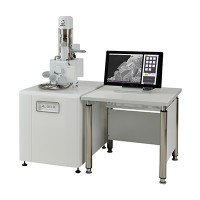
JSM-7200F Schottky Field Emission Scanning Electron Microscope
- Post on 27-03-2019 02:25:55 AM - 5566 Views
-
JSM-7200F has much higher spatial resolution than the conventional models at both high and low accelerating voltages by applying the technology used for “In-Lens SchottkyPlus”, the electron optics equipped on our flagship-model, JSM-7800FPRIME, and by incorporating TTLS (Through-The-Lens System). The maximum probe current of 300 nA is also guaranteed because of the above mentioned features. Thus, JSM-7200F is a next-generation multi-purpose FE-SEM that has capability of high resolution observation, high throughput analysis, ease of use, and expandability.


In-Lens Schottky Electron Gun
The In-Lens Schottky electron gun (JEOL patented) has been developed by optimizing the geometry of the electron gun and the low-aberration condenser lens. By this unique technology the electrons emitted from the electron gun can be utilized efficiently than the conventional one, so smaller-diameter of electron probe even with large current is possible. Thus, JSM-7200F is capable of high throughput analysis (EDS, WDS, EBSD, etc.).
TTLS(through-the-lens system)
TTLS (through-the-lens system) is a system that enables high resolution observation at low accelerating voltage and also selection of different signals generated from the specimen by using GB (Gentle Beam mode).
By applying bias voltage to the specimen with GB (Gentle Beam mode), the incident electrons are decelerated and the electrons emitted from the specimen are accelerated, so it is possible to have high resolution images with better signal-to-noise ratio even at low accelerating voltage/landing voltage.
The filtering voltage of the energy filter equipped on TTLS enables you to control the amount of secondary electrons to be detected by the upper detectors. Therefore, images of the top surface of the specimen generated only by high-angle backscattered electrons can be observed at low accelerating voltage with the upper electron detector (UED).
Low-energy electrons, which are not detected with UED and pushed away by the filtering voltage, can be also detected with an optional upper secondary electron detector (USD). Thus, JSM-7200F can detect both secondary electron image and backscattered electron image simultaneously.
Hybrid Objective Lens (combination of magnetic-lens and electrostatic-lens)
JSM-7200F adopts a newly-designed objective lens called “hybrid lens”.
The hybrid lens combines a magnetic-lens and an electrostatic-lens in order to reduce aberrations, so it is possible to obtain higher spatial resolution compared with the conventional out-lens. JSM-7200F also keeps the usability of the conventional out-lens, so it is no problem to observe and analyze magnetic samples.
Applications
Data taken by using the hybrid lens and GB (Gentle Beam mode)
The low-aberration hybrid lens and GB (Gentle Beam mode) enables high resolution observation of insulating materials at very low accelerating voltage.
 ×40,000
 ×150,000
Landing voltage: 0.5 kV
Specimen: Mesoporous silica (Courtesy of Professor Shunai Che, Shanghai Jiao Tong University, China)
Data taken by the upper electron detector (UED) with an energy filter
These images are taken by UED at low accelerating voltages. These are high-angle backscattered electron images with composition-rich information, but the image taken at 0.8 kV shows much finer structures of the top surface compared with the image taken at 5 kV. It is necessary to have not only the upper electron detector (UED) but also an energy filter to obtain backscattered electron images of the top surface in order to cut out secondary electrons.


Accelerating voltage: 0.8 kV(to the left), 5kV(to the right)
Energy filter: -250 V
Specimen: The surface of an Au plate


-
Unparalleled Stability...
27-03-2019 01:38:04 AM -
The Reference Machine in...
27-03-2019 01:28:20 AM -

SMALL PARTS COUNTER U-60
27-03-2019 01:04:31 AM
- HCMC Office: Block A, Lever 2, Linh Trung Building, No 6-8, Road no 16, Linh Trung Ward, Thu Duc City, HCMC.
- Head Quaters: 427 Le Dai Hanh, Ward 11, District 11, HCM City.
- Hanoi Office: 156A Quan Thanh Str., Ba Dinh Dist., Hanoi City.
- Phone: +84-28-66865303
- Mobile: +84 982 427 168
- Email: dung@ngocminh-ise.com
- Website: http://ngocminh-ise.com